Infrequent Investment Ideas Vol.2: Why Buy TSMC’s Stock (TWSE: 2330)?
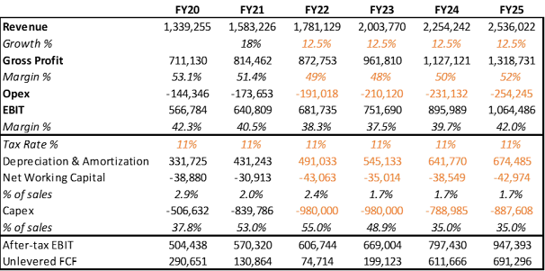
TSMC’s management raised their guidance for FY21 revenues on the 2Q21 earnings call and told investors that they expect revenue growth through 2025 to be towards the higher end of the earlier provided range of 10-15%/year. This will require investments of $100bn through FY23, which will be TSMC’s most intense investment period this century, not only in absolute terms but also relative to sales. Management, nevertheless, discussed maintaining or even improving (average) profitability through FY25. If this guidance is met, TSMC will logically compound EBIT at 10-15% during the next 4 years to NT$1.064bn at mid-point. Depending on one’s assumptions about capital intensity after FY23, unlevered free cash flow could more than double from the FY20 level.
Exhibit 1: My estimates of TSMC’s
operating results in FY20-FY25 (in NT$m) implied by guidance; assumptions are
in orange
If those investments generate
returns similar to what TSMC has averaged over the past 10 or even 20 years (25%
average RoIC[1] over the past 10 years, 23%
over the past 20), the FY25 guidance is not only within reach but appears disappointing.
TSMC’s management are among the industry’s best, and they don’t make such bold
predictions often. Considering the cyclical/volatile nature of the
semiconductor industry, this guidance is indeed bold in terms of both its
duration and growth rate. Rosy as these predictions might seem, they likely
understate management’s real expectations. This sounds speculative, but the
industry’s technology roadmap and TSMC’s positioning in the industry lend this
guidance a lot of credibility.
For most of the past 10 years,
TSMC’s stock traded at around 14x EV/NTM EBIT, until FY19, when it became blindingly obvious that Intel’s
10nm problems have set it back years (the number is up for debate) behind TSMC
in terms of manufacturing capabilities. Intel’s sole competitor in x86
CPUs, AMD, has since been enjoying TSMC’s process advantage, gaining share in
consumer CPUs and making inroads in the server market.
The pandemic-induced boom in
compute demand and the 5G ramp then propelled TSMC to 25% revenue growth in
FY20, marking the company’s fastest growth since FY14, when TSMC replaced
Samsung as Apple’s fab of choice for the iPhone processor. TSMC’s stock
continued rerating up, and it started FY21 trading at ~26x EV/LTM EBIT after
TSMC reported 4Q20 results. It then sold off a bit and has traded at ~20x
EV/LTM EBIT for most of this year, despite management’s FY25 guidance
announcement and the raise of that guidance on the 2Q21 call.
The achievement of management’s
guidance would probably mean that TSMC has extended or at least maintained its
technological lead over Intel and Samsung. This, in turn, would imply plenty of
opportunity for growth beyond FY25 (maybe a bit slower considering the FY25
base). So, what would TSMC be worth then, and, hence, what is it worth now?
Exhibit 2: TSMC’s EV/NTM EBIT over
the past 10 years

The below table summarizes the
potential values for TSMC’s EV at the end of FY24, depending on what multiple
the market would ascribe to its FY25 EBIT of NT$1.064bn. This, of course, would
be dependent on a few factors, including the interest rate environment, but
companies in quasi-monopoly positions in industries with secular tailwinds rarely
get optically cheap. At 25x-30x FY25 EBIT, TSMC’s FY24 MV would offer 19-27%
compounded annual returns, not even factoring in dividends (historically ~50%
of net income). At the risk of stating the obvious, this is a fantastic rate of
return, so why hasn’t at least some of it been arbitraged away?
Exhibit 3:[2]
Future value of TSMC’s FY24 MV (in NT$m) and implied compounded return from
current MV

It appears the market is
currently placing fairly low odds on the company meeting its guidance, and we
need to understand why. To do this, first we must answer the question, “What
needs to happen for TSMC’s guidance to be met?” Though this is a bottom-up
fundamental analysis memo, some top-down thoughts would help us arrive at the
answer in broad strokes.
TSMC is the world’s largest
foundry with ~55-60% market share and is close to a monopoly in leading-edge
foundry services. Foundry demand is driven by the broader semiconductor market.
TSMC’s growth in any given year has long been entirely driven by revenues from
what were at the time leading-edge processes, with lagging-edge processes
typically declining year-on-year (2021 is a bit abnormal). Since TSMC’s share of
the foundry industry exceeded 50% in 2014, it follows that TSMC’s leading edge
growth has accounted for more than half of the foundry industry’s growth. This,
of course, makes sense in the context of Moore’s Law. The table below summarizes
the growth trends of the semis and foundry industries over the past 20 years.
Exhibit 4: Growth trends of total
semiconductor sales and foundry sales

So, the conditions sufficient/required to be met for TSMC’s guidance to be realized would be:
1) The semiconductor industry, and the leading-edge subset in particular, continuing to grow at a rate similar to its 5-year CAGR for the next 5 years;
2) TSMC at least maintaining its current market share of the foundry market and the leading-edge subset in particular;
3) TSMC continuing to deliver enough value to its customers to at least maintain its current economics/profitability profile.
Therefore, the substantial gap
between price and value suggests the market is pricing all three being met as less
than likely. Though the semiconductor industry has historically been cyclical
and will most probably continue to oscillate between boom and bust, and the
current shortage will probably turn into a glut at some point, the secular
trends[3]
arguably accelerated by the pandemic incline me to believe that the market is
not discounting 1) as unlikely. Discussing 1) would be too much of a top-down
endeavor or an overwhelming collection of bottom-up tasks for each large
semiconductor company and so 1) is ticked off as quite likely for the purposes
of this analysis. Then the risks to 2) and 3) can be distilled to:
- Intel, Samsung, SMIC, and/or an upstart foundry
catching up to and/or surpassing TSMC in technological capabilities and gaining
share of the leading-edge foundry market by offering a better value proposition
to customers;
- Geopolitical calculations altering the semiconductor fabrication landscape either through preferential treatment for domestic foundries in the U.S. and Europe or an outright Chinese invasion of Taiwan.
Assessing the likelihood of 2)
and 3) transpiring is very much a bottom-up process. The rest of this memo
discusses some recent industry developments and TSMC’s competitive advantages
(with references to Hamilton Helmer’s “Power” framework), which, taken together,
inform my hypothesis that the risks listed above are unlikely to pose a
significant threat to the FY25 guidance being met or exceeded and that TSMC
would be able to fend off any additional threats should they arise. This would
make TSMC’s potential EV in the next few years (and its present value today)
quite attractive relative to the current stock price.
Semiconductor Capital Intensity/The End of Moore’s Law
Over the past 20 years, semiconductor revenues and silicon shipments have moved in lock-step, while transistor (silicon area) density, performance, and power efficiency have improved roughly as predicted by Intel co-founder Gordon Moore. The increase in transistor density has meant that a consistent price/square inch of silicon translated to lower price/transistor, better performance/watt, or simply higher and more energy-efficient performance per dollar.
Exhibit 5: Industry revenues (in $m)
and silicon shipments (in millions of square inches)

However, the physics problems to
be solved for this progress to continue have been increasing in difficulty.
Hence, Moore’s Law’s progress has been predicated on increasing R&D investments
on the part of wafer fabrication equipment (WFE) manufacturers, which, combined
with the industry’s cyclicality, has been a spell for consolidation. Today, the
top 5 companies (Applied Materials, ASML, Lam Research, Tokyo Electron, and
KLA) account for 2/3rds of WFE revenues and spent $8.4bn on R&D in CY20,
about 2% of the entire semiconductor industry’s revenues. These companies have
held the keys to improving performance and, hence, charge sufficiently high
prices to earn great returns on these R&D investments.
The rising costs of
manufacturing, coupled with the cyclicality of the industry, dissuaded a lot of
the IDMs from participating in leading-edge manufacturing, and foundries picked
up the capex tab but also claimed a larger pie of industry revenue to be compensated
for their troubles.
Exhibit 6: Wafer Fabrication
Equipment and foundry sales as % of total semiconductor revenue

As a result, for the past 5 years
or so, as improving transistor density has been approaching its physics
limitations,[4]
the rate of performance improvement has slowed below the rate predicted by
Moore’s Law, and these slowing improvements have been increasing in cost.
The higher equipment bills and
the slowdown of transistor scaling have, logically, led to an increase in the
cost per transistor at the leading edge.
Exhibit 7:[5]
Transistor costs are rising

There is further nuance to
equipment costs – a significant amount (as much as 95%[6])
of tools used in one process node can be reused in the next process node
(lowering costs), but the leading-edge foundries are also adding capacity
(increasing costs), and every new node has required more processing steps,
requiring more/newer/more expensive equipment to achieve the same
throughput/capacity (increasing costs). Of course, with the introduction of EUV,
the degree of equipment reuse has decreased significantly. On balance, each new
node has proved more expensive for foundries.
Exhibit 8: Relative production costs
by process node

Exhibit 9: My estimates of greenfield
capex per 1,000 wafer starts per month of capacity

Source: TSMC, Applied Materials, SIA, Tokyo Electron, DigiTimes
The discussion of manufacturing
costs has so far focused on the challenges and costs of fitting more
transistors on a square millimeter of silicon and, hence, the front end of
manufacturing. The back end, namely packaging, has long been a performance
bottleneck, perhaps overlooked because of the reliable performance improvement
in accordance with Moore’s Law at the front end. At the risk of oversimplifying,[7]
this limitation stems from the necessity of chips to communicate with other
chips through metal interconnects and substrates, and the improvement in the
density of those has significantly lagged transistor scaling. The industry has
turned to packaging for the next wave of performance improvement, as transistor
scaling nears its physical limits. Advanced packaging techniques have provided
vital alternatives to large monolithic dies (with all the associated
manufacturing issues at advanced nodes) in computing (chiplets used by AMD and
Intel) and enabled revolutionary antenna technologies for 5G devices.
Historically a small sliver of
WFE (typically <10%), back-end equipment is becoming an increasingly
important corner of semiconductor manufacturing equipment. There are two pieces
of good news for foundries: 1) packaging is becoming more tightly coupled with the
front-end of manufacturing[8]
in which foundries specialize, and 2) advanced packaging could bring the next
wave of performance improvement beyond Moore’s Law.
Exhibit 10: The next decade in
manufacturing, according to a major advanced packaging equipment manufacturer

The bad news is that its costs
are incremental and not a substitute for front-end equipment.
Exhibit 11:[9]
Relative production costs by process node, front-end and back-end

The rising WFE bill has caused
consolidation at the leading-edge after Globalfoundries bowed out of the race
to 10nm. Today, only a handful of players are willing and able to pay the
eye-watering equipment bills for production capacity at the leading-edge (and
make it work): Intel, Samsung, and TSMC, with Intel struggling to catch up to
Samsung and TSMC. Of these, TSMC is the only pure foundry and arguably (Samsung
would argue) has the most advanced process in what it calls 5nm.
Exhibit 12: Share of non-memory wafer
production by process node

Exhibit 13: Top two companies’
spending as a % of total WFE sales

The challenge that foundries are
facing is delivering enough value to customers through silicon performance
improvements at an acceptable yield in order to charge wafer prices sufficient
to earn an attractive return on the ever-increasing investments required at the
leading edge.
TSMC’s Competitive Advantage #1: Shared Scale Economics
Pricing
TSMC is not maximizing profits.
Articles about TSMC’s 20% in wafer prices often fail to mention the costs
involved in building out capacity for these wafers. One could argue that TSMC
earned the right to extract huge value from its customers, since TSMC put a lot
of capital at risk to push the envelope of leading-edge manufacturing and build
out capacity, but that’s not consistent with TSMC’s business philosophy. The
company’s management has taken a different path. They refer to customers as
partners and explain their pricing decisions as “strategic, not opportunistic.”
Management has long realized the value of co-developing processes with
customers and that such collaboration and opportunistic pricing are not
congruent.
This is clear from a quick look
at TSMC’s financial statements – RoIC has been relatively stable over the past
20 years, even as the company has become the clear leader at the leading edge.
The benefits from TSMC’s superior processes and economies of scale are
shared with customers to assure an industry-leading value proposition.
The years of slightly higher
returns preceded periods of substantial investments, so the profits made in
those higher return periods were used to finance the increased capital
expenditures (TSMC has maintained net cash positions for at least the past 20
years). This has been well understood by leading-edge customers, such as Apple,
for whom an industry-leading technology roadmap, supported by sufficient
capacity, is a key aspect of suppliers’ value proposition.
Apple, for example, does not have
an alternative to TSMC at 7nm and below. Apple initially left Samsung because
Samsung is its major competitor and was tempted to take a peek at its IP. This
dynamic is extant today but is no longer the only reason Apple has stayed with
TSMC as its sole manufacturer of the A-series processors. Samsung could
arguably no longer provide the same performance at the leading-edge, does not
have sufficient capacity for external customers, and lacks the packaging
processes Apple co-developed with TSMC. TSMC could charge Apple a lot more than
$17-20k[10]
per wafer at 5nm… at least for a few years.
A deeper look into the customer
relationship with Apple would serve well to illustrate the value TSMC offers to
its customers, derived from its shared scale economics strategy.
Apple is usually the first
customer of TSMC’s latest process node. TSMC sent hundreds of engineers to
Cupertino in 2013 to work with Apple on its transition from Samsung’s foundry
services.[11]
This close collaboration has continued ever since, and Apple is an important
contributor to key parts of the technology development. Apple has a very big
incentive to make these contributions, considering the leading-edge capex
requirements discussed earlier – it simply wouldn’t be feasible for Apple to go
completely vertical and manufacture its own chips, unless it’s prepared to lose
money in the endeavor.
Here’s why.
Assuming one knows the die size
of an A-series processor, the iPhones’ (and now Macs’) workhorse processor, the
process node on which it is manufactured, and the die’s yield, one can make enough
estimates to illuminate the economics faced by TSMC and Apple and, therefore,
to assess who gets what value in the relationship. These estimates, however,
rely on a number of assumptions and so are only as good as those assumptions,
but hopefully the logic behind both assumptions and estimate calculations is
sound.
Let’s take the A14 and A15
processors of the iPhone 12 and 13 series, respectively, which are both manufactured
on TSMC’s 5nm process. Some public data[12]
on TSMC’s 5nm defect rate/cm^2, which is a key component in yield calculations
(to be discussed in more detail later), reveals that 5nm initial defect rates at
high volume manufacturing were actually better than 7nm ones, and the rate of
yield improvement was comparable, so TSMC probably achieved better initial
yields on the A15 processor, despite its larger die size. Net, TSMC probably
managed to squeeze more A14s out of a wafer on the 5nm process due to the
smaller die size.
Estimates of unit sales of the
iPhone 13 (not mine) suggest it would be selling better than the iPhone 12 in
the holiday season. Here comes a key part of the TSMC-Apple relationship. Demand
for the latest iPhone is seasonal and fleeting, but TSMC needs to build enough
capacity to satisfy that peak demand. It appears the A12 sold about 60m units
in 4Q20, which I assume means TSMC had had to build peak capacity for 40
million phones (pre-building some inventory). If the A13 does sell 80 million units
(as rumored) in calendar 4Q21, TSMC probably needs to have built peak capacity
for 55 million phones. It’s evident from earnings calls that peak capacity
planning is top of mind for management, and I’ll discuss the reason shortly.
Exhibit 14: My estimates of A14 and
A15 peak capacity needs; assumptions are in orange

The table above suggests that TSMC must increase capacity by
37.5% for the iPhone 13, but since iPhone sales are seasonal and dominated by
the newest models in the quarters of and following their release, the iPhone 12
will require significantly less than peak capacity after iPhone 13’s release. Assuming
that after 2022 the iPhones 12 and 13 decrease in volume at a rate similar to
that of the iPhone 11, one can estimate wafer demand in the next 5 years, which
is the period that TSMC uses as the equipment’s useful life in accounting for
depreciation.
Then, using the capex/1,000 wafer starts per month (kwpm),
one can estimate how much TSMC must spend to build out this capacity. TSMC
plans to spend about $400m/kwpm to build out its 5nm fab in Arizona. However,
the Arizona fab buildout will be starting from scratch (greenfield). TSMC’s 5nm
capacity in Taiwan uses a lot of existing infrastructure, as well as a
significant amount of 7nm tools (about 90% of tools can be repurposed, per
TSMC’s comments). EUV is a larger part of the 5nm process, so there is still a
significant incremental investment. I assume $200-$250m/kwpm. Finally, using
TSMC’s disclosure, one can estimate labor costs and variable costs/wafer. The
results are summarized in the table below (continues on the next page).
Exhibit 15: Illustration of TSMC’s
iPhone 12 and 13 economics excluding opex; assumptions are in orange

This analysis is for illustrative
purposes only, and all corrections are welcome. It aims to illustrate that TSMC
takes on the huge costs of building out sufficient capacity for Apple, who only
use the full capacity for no more than two quarters. The result is that TSMC
will be burning a significant amount of cash in the first two years (and this
is before considering opex) unless it finds enough customer demand to
fill the capacity after satisfying Apple’s peak demand. Any miscalculation in
peak capacity planning costs dearly. Foundries live and die by yield and
utilization, and how utilization impacts per wafer economics is illustrated
below (opex excluded from cost assumptions and estimates).
Exhibit 16: Illustration of wafer
unit economics, excludes opex

With each new node, it appears TSMC sets a new record for
the number of customers it has secured on the node. These customers’ products
also target a diverse set of applications and end-markets – from smartphone
processors and notebook CPUs to specialized AI and crypto mining data center
processors. Thus, wafer demand volatility is smoothed out to an extent. This
allows TSMC to plan accordingly and set wafer prices at levels that offer such
value to each customer that it makes it really hard to think of how a rival can
compete. Using the data presented above, I estimate that Apple pays ~$40-50
per chip for A15, which powers a phone whose (rumored) bill of materials is
~$500 and is selling for >$1,000 – shared scale economics at work.
Competitive Advantage #2: Process Power/Superior Technology
I discussed one of the two major
operational factors dictating a fab’s profitability, namely utilization. The
other one is yield. Fitting square chips on a circular wafer means that a
portion of the wafer is lost at the edges. Additionally, each step of the
manufacturing process faces some probability that a defect occurs somewhere on
the wafer. A defect renders the chip on which it occurred (at least partially)[13]
useless. The wafer’s yield is the percentage of the wafer area that is defect-free.
The yield of a chip (or die) is the number of defect-free (good) chips as a
percentage of the maximum number of chips that can theoretically fit on a
defect-free wafer. A larger die size means fewer chips can be fit on a wafer,
so one defective chip represents a larger percentage loss (compared to a
smaller chip). Hence, chip yield and chip die size are inversely related for a
given defect rate.
Exhibit 17: Basic die yield equation

Source: From the book Extending
Moore’s Law through Advanced Semiconductor Design and Techniques
Wafer purchase agreements between
foundries and their customers are confidential and differ from customer to
customer, but all customers are in the business of selling or using
non-defective chips, so these agreements usually stipulate a minimum acceptable
yield. If the foundry fails to deliver, it has to make the customer whole
through either monetary compensation or extra wafers. In effect, the customer
wants to guarantee the delivery of a certain number of chips for its money
(price/chip). Volume discounts are also features of the typical wafer purchase
agreement.
The basics of yield economics are
summarized by the equation below. It simply formalizes the fact that a foundry will
have to process more wafers to deliver the same number of chips (earn the same
revenue) as a foundry achieving better yield.
Exhibit 18: Basic relationship between
wafer cost and die yield

Of the variables in the basic
yield equation, the one that’s within a foundry’s control is the defect rate. Minimizing
defect rates has a learning curve for each node, and since the majority of
tools used in a given node can be repurposed for the next node, the learnings
cumulate across nodes. Hamilton Helmer would term this hysteresis – “[the]
process advances are difficult to replicate, and can only be achieved over a
long time period of sustained evolutionary advance.”[14]
Not only is leading-edge yield a
product of hysteresis, but the difficulty of achieving it at every node is
growing exponentially. Referring back to the die yield equation, die yield is
decreased by each additional critical mask layer (through a power law), and
each mask layer requires several processing steps. The figure below illustrates
the rise in the number of processing steps at leading-edge nodes. Whether the
defect rate at each processing step is probabilistically dependent on or
independent of other steps, each step entails some probability of a defect
occurring. To achieve yields of 90% at 5nm, a foundry must execute more than
1,000 incredibly sophisticated processing steps near perfectly, and this is
exactly what TSMC does.
Exhibit 19: Number of process steps
per wafer at the leading-edge

Source: Fabricated Knowledge, CMC
Materials Investor Day
What’s even more impressive and terrifying for competitors is that the accumulation of manufacturing expertise in one node often helps achieve better yields on the next one. The learning curve for TSMC’s 7nm and 5nm processes is illustrated below.
Exhibit 20: TSMC’s 7nm and 5nm defect
rate progression

Advanced packaging[15]
is not a substitute for front-end complexity at the leading edge but rather
layers on additional complexity. Manufacturing smaller leading-edge chips
(chiplets) to package together might improve individual die yields and costs,
but packaging the chiplets also has a yield of less than 100%. Additionally, manufacturing
two different chips with yields of 90% each are probabilistically independent
events and packaging them together has a yield of 81%, on average, even if you
assume 100% packaging yield. For sophisticated computing chips with large die
sizes near the reticle limit, large monolithic chips might not be feasible at
all, so advanced packaging of chiplets might be the only solution.
Advanced packaging is analogical
to the leading-edge in the back-end, and it has its own engineering challenges,
more mechanical than chemical/optical when compared with the front-end. TSMC is
well on its hysteresis path in advanced packaging as well after pioneering
fan-out packaging (InFO) of logic in high volume with Apple back in 2016.
Finally, there is the issue of
cycle times or throughput.[16]
RoIC is the product of asset turnover and operating margin, and wafer capacity
is similarly a product of throughput and yield. Therefore, the return on the
huge equipment investments discussed earlier is a function of both yield
(non-defective chips/wafer) and throughput (wafers processed/unit of time).
A semiconductor fab is a collection
of numerous tools from various vendors. Each tool has a maximum theoretical
throughput, and it’s the foundry’s job to get as close to that throughput within
a certain defect rate envelope. Processing times per mask layer vary between
foundries, and the best foundries take 20-50% less time than average or
below-average foundries. These time savings really add up at the leading edge with
the large number of steps involved.
However, according to ASML, the
biggest contributor to cycle times is the wait times between steps. Wait times
also tend to increase with fab utilization. Consequently, process flow
automation and optimization can be real differentiators in productivity and
cost. These, like front-end and back-end defect rate optimization, are also the
result of years of accumulation of expertise or hysteresis.
Competitive Advantage #3: Counter-positioning/Revolutionary
Business Model
This one is fairly
straightforward and well-understood but is hugely important and so merits a
brief discussion. As the world's first pure-play foundry, TSMC had a unique
proposition when it was founded in 1987 - we will only manufacture the chips
you design and will not compete with you by designing and manufacturing our own
chips. The Apple-Samsung IP incident reveals how important this is for
protecting IP. Nvidia and AMD are two of TSMC’s customers who begin using
TSMC’s most advanced process not long after Apple. It’s tough to see what
compels them to use Intel’s foundry services despite all of Intel’s assurances
that the foundry business will be a walled-off entity, separate from Intel’s
own chip business.
Then there is the issue of
capacity prioritization. The pandemic drove huge demand for both consumer and
server CPUs. Would AMD trust Intel Foundry Services to honor its wafer
obligations when Intel’s internal production capacity is running full, and the
mothership is missing out on the unforeseen revenue windfall? Would Intel want
to include adjustable wafer prices in the wafer purchase agreements to be
compensated in such events, and why would AMD sign such a contract? The same
logic broadly applies to Samsung and its chip competitors as well. These are
just some of the questions that the conflicts of interest involved in Intel’s
and Samsung’s foundry ambitions raise.
And if Intel and Samsung are
unable to attract at least some of their competitors as customers, how would they
enlist enough customers and secure enough demand to make the peak capacity
economics discussed above work? And if they can’t make the economics work, how
can they offer low enough prices to have a better or at least comparable value
proposition compared with TSMC’s and so forth.
Competitive Advantage #4: Network Effects
Network effects are usually
associated with Internet platforms, but, effectively an aggregator of leading-edge
demand, TSMC benefits from them, too. “Network effects” simply means the value
of a product or service to each customer increases with the number of customers
using it. There are several network effects in TSMC’s foundry services. First,
the wafer economics described in the shared scale economics section are made
possible by the number of customers whose orders fill the newest node capacity
built for peak Apple demand.
Network effects also exist in the
sophisticated IP ecosystem which TSMC built over the past ~15 years. Once the
initial design is complete, every chip design needs to be qualified for
production, and that process’ complexity increased with the advance of Moore’s Law.
To speed the process up, TSMC launched the Open Innovation Platform (OIP) in
2008. Essentially, it was a library of design kits, IP blocks, and other design
tools, which TSMC had qualified for its design rules.
Shortly thereafter, it also
launched its CyberShuttle service (which it copied from a US academic idea). It
was the industry’s first multi-project wafer service – companies would send
their mask designs to TSMC, and TSMC would use them to produce many different
chip designs on the same wafer, cut the chips up, and send them back to the
customers for verification; this would greatly reduce mask design costs as
compared to having each company using separate wafers with their own masks for
their prototypes.
CyberShuttle directly reduced
design costs, while OIP reduced time-to-market, which is a real economic cost
for customers.
Both of these initiatives were
copied by competitors, but TSMC had the first-mover advantage. Design software
tools companies like Cadence and Synopsys and IP companies like ARM had the
incentive to work with TSMC to have their tools and IP qualified for TSMC’s
processes, given its large customer base, and new customers or existing
customers expanding product lines chose TSMC for the lower design costs and
short time to market, and so the cycle went. TSMC is today at the center of an
ecosystem of IP companies, design tools makers, front-end and test and
packaging equipment suppliers, and fabless companies. As a result, it has the
broadest IP library and years of learning and co-development of various chips.
Before TSMC’s business model
disrupted the semiconductor industry, IDMs were mostly manufacturing
proprietary chips (they did have some foundry services), so they developed expertise
in the manufacturing of the types of chips in which they specialized. TSMC opened
its doors to all companies and so produced chips with various architectures and
die sizes for a diverse set of applications. Again, this was copied as competitor
fabs emerged, but TSMC again had the first-mover advantage. This exposure
probably helped TSMC with establishing its most important competitive advantage
(together with its shared scale economics pricing philosophy) – its ability to
achieve economically viable yields on industry-leading technology processes.
Conclusion
In the first section of this
memo, I listed what I think are the major risks to TSMC’s business, risks that
could prevent it from achieving its FY25 guidance. After discussing TSMC’s
competitive advantages, I will now briefly discuss why I think these advantages
render the probability of these risks unfolding:
- Intel, Samsung, SMIC, and/or an upstart
foundry catching up to and/or surpassing TSMC in technological capabilities and
gaining share of the leading-edge foundry market by offering a better value
proposition to customers;
Though TSMC spent $3.7bn on
R&D in 2020 (44% more than the largest spender among WFE companies, ASML),
some of its most valuable IP is the product of years of learning from
experience and cannot be found on the balance sheet. But it is an asset that
enables TSMC’s leadership. While a lot of the R&D burden is shared with
customers who make significant contributions to the development of new processes,
TSMC’s manufacturing expertise is a very opaque IP asset that is next to
impossible to reverse-engineered.
Intel and Samsung are
leading-edge powerhouses, as well, but TSMC is a few steps ahead, and that
advantage is difficult to surmount in a hysteresis-driven process. Indeed, TSMC
surpassed Intel, but it took a few years after Intel made the fateful decision
not to use EUV (it has since reversed course). It is possible that TSMC makes a
similar mistake in the future (maybe it’s a mistake to continue to rely on
FinFET transistors as Intel is pushing GAA), but I think its customers have the
incentive to help steer its technology roadmap in the right direction not only
because they face not insignificant switching costs, but also because these
customers are reluctant to use the foundry services of competitors, as
discussed earlier. For now, the rumored negotiations between Intel and TSMC for
Intel to secure capacity at TSMC for its GPU chiplets are a testament to TSMC’s
lead.
Intel is currently mounting an
attack from a position of weakness. The company is now past the stage of denial
about its manufacturing capabilities and has entered the panic phase. Aside
from its technological inferiority and conflicts of interest, there has always
been another problem with Intel’s foundry operations that the company is now
forced to face – Intel has been running at close to 25% free cash flow margin, with
its operating cash flow margin at ~45%. The implication is that Intel is now
facing a much higher capex bill than anything seen in recent memory. Intel’s
gross margins have been a few percentage points above TSMC’s (high 50%s), even
as it has enjoyed lower depreciation/sales. It’s tough to see how Intel doesn’t
take a significant hit to profitability even when its foundry operations
mature. On the other hand, it’s tough to see how Intel reverses the process of
losing share in CPUs to AMD and Apple in the consumer segment, and AMD and all
the hyperscalers in the server segment, and how its core CPU business regains
importance as new computing needs increasingly demand new architectures. Intel
seems to be forced to go all in on the foundry business.
Other competitors, such as
China’s national foundry champion, SMIC, are living proof that simply throwing
money at the problem of achieving economically-feasible yields at the leading
edge is no solution. SMIC is many years behind Intel, Samsung, and TSMC,
despite the seemingly endless subsidies, government incentives, and the constant
influx and exodus of elite managers. The US embargo on EUV tools won’t exactly
help China’s cause either.
- Geopolitical calculations altering the
semiconductor fabrication landscape either through preferential treatment for
domestic producers or an outright Chinese invasion of Taiwan;
Intel’s CEO, Pat Gelsinger, is,
among semiconductor executives, the most vocal proponent of government support
for U.S. semiconductor manufacturing. Mr. Gelsinger preemptively criticized the
future U.S. support TSMC might receive for its Arizona fab, but TSMC’s Arizona
fab plans, which assume some government support, suggest the U.S. government is
more concerned with the geographical location of the fabs than with who their
owner is (as long as it’s not Chinese, of course). TSMC’s management on several
occasions stated that there is no way a US fab can match the economics of its
Taiwan complexes, so government incentives will have to be substantial.
Even with substantial government
support not available to TSMC, Intel and Samsung will still be facing
competitive disadvantages in technology and business model. Government
incentives might solve the capital intensity problem for Intel, but they won’t
solve the technological problems. Western governments also move slowly,
especially when it comes to big spending bills, and meanwhile TSMC will be advancing
ahead.
Lastly, the risk of China
invading Taiwan seems to have increased in the minds of Western leaders. This
would be, as Jon Stokes puts it, “a catastrophe for China and the world,” primarily
because of the potential crippling of TSMC. He explains very well why in this
article: https://www.jonstokes.com/p/why-a-chinese-invasion-of-taiwan. When asked about the risk to TSMC
of a Chinese invasion, one investor/analyst stated that the investment
portfolio wouldn’t be top of mind in such an event, the implication being that
the invasion would presage World War III. After reading Jon Stokes’ article,
one could envision a more nuanced set of outcomes, though it would be safe to
say that the value of TSMC’s business would be significantly and almost
certainly negatively impacted by a China invasion. But I also think that this
is a very top-down risk, whose probability is very difficult to accurately
estimate, especially by equity investors, and the overestimation might be
behind some of the gap between price and value.
Martin A.
[1]
RoIC = EBITt*(1-Tax Rate)/((Invested Capitalt + Invested
Capitalt-1)/2); Invested Capital = Total Assets – Cash &
Equivalents – Payables
[2]
Assumes 50% Dividend Payout Ratio (as % of Net Income) in FY22-FY25; ignores
dividend in Compounded Return calculation
[3] All
the buzzwords – 5G, AI, Autonomous Vehicles, EVs, cloud migration etc.
[4] https://www.technologyreview.com/2021/10/27/1037118/moores-law-computer-chips/
[5]
Gate costs can be used as a proxy for transistor costs
[6]
Per TSMC’s earnings calls
[7]
See SemiAnalysis for a very informative introduction to advanced packaging: https://semianalysis.substack.com/p/advanced-packaging-part-1-pad-limited
[8] As
evidenced, for instance, by the partnership between Applied Materials and BE
Semiconductor
[9]
FEOL = Front-End Equipment; BEOL = Back-End Equipment
[10] These
prices circulate on the internet and are somewhat backed by my wafer $ASP
estimates in Exhibit 10
[11] https://www.wsj.com/articles/tsmc-starts-shipping-microprocessors-to-apple-1404991514
[12]
Presented at the TSMC Tech Symposium 2021
[13]
Logic chips, for example, are still sold if some of the chip’s cores are
defective/non-functioning; they are simply sold at the price of chips with a
lower core-count, according to how many cores are functioning.
[14] 7 Powers: The Foundations of Business Strategy by Hamilton Helmer
[16]
For a very informative discussion of cycle times: https://semiengineering.com/battling-fab-cycle-times/.
The throughput discussion mostly used this article as a reference.

Коментари
Публикуване на коментар